Sommige informatie wordt in het Engels weergegeven.
Over mij
Hello,
I’m Benjamin Lewis, a professional PCB Design Engineer specializing in high-quality circuit board design and manufacturing files.
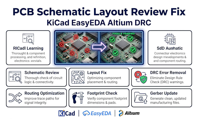
I create clean, efficient, and production-ready PCB designs from simple single-layer boards to complex multilayer layouts. Using industry-standard tools like KiCad, EasyEDA, and Altium Designer, I deliver accurate schematics, optimized PCB layouts, Gerber files, BOMs, and full manufacturing documentation.
My focus is on designs that are reliable, cost-effective, and ready for immediate fabrication.... Lees meer