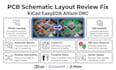
I will review fix pcb schematic layout kicad easyeda altium drc

Sommige informatie wordt in het Engels weergegeven.

Verenigd Koninkrijk

Ik spreek Engels, Duits, Spaans, Frans, Italiaans

ELECTRICAL ENGINEER

Hello, I’m Benjamin Lewis, a professional PCB Design Engineer specializing in high-quality circuit board design and manufacturing files. I create clean, efficient, and production-ready PCB designs f...
Over deze dienst

I will review and fix your PCB schematic and layout using KiCad, EasyEDA, or Altium Designer.


If your board has errors, DRC issues, routing problems, grounding faults, or manufacturing risks, I will analyze the design and correct it for reliable performance and fabrication readiness.


Avoid costly manufacturing mistakes. Get your PCB verified and optimized before production.


What I Offer:

  • PCB Schematic Review
  • PCB Layout Review
  • DRC Error Fix
  • ERC Check
  • Routing Optimization
  • Component Placement Fix
  • Ground Plane Optimization
  • Trace Width Correction
  • Clearance Adjustment
  • Footprint Verification
  • Multilayer PCB Review
  • KiCad Support
  • EasyEDA Support
  • Altium Designer Support
  • Manufacturing Optimization


What You Will Get:

  • Detailed design review report
  • Fixed schematic files
  • Corrected PCB layout
  • DRC clean design
  • Improved routing structure
  • Updated Gerber files if required
  • Optimization suggestions


Contact me now to place your order!

Specialisatie:

Circuit design

Schema's

Lay-out

Voetafdruk

Bestandsformaat:

Gerber

STEP

VRML

SCH

PDF

Software:

Altium ontwerper

Eagle CAD

EasyEDA

KiCad

AutoCAD

arduino

Interface:

HDMI

MIPI DSI/CSI

I2S

TDM

UART

USB

SPI

I2C

SDIO

PCIe

BT