Door categorieën bladeren
Ontdekken
Fiverr Pro
Nederlands
$
USD
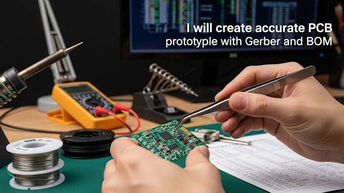
PCB Prototype Engineer Schematic Layout Expert
I specialize in creating accurate and professional PCB designs using EasyEDA and KiCad. With expertise in electronics engineering, I deliver complete PCB prototypes with Gerber files, bill of materials (BOM), and detailed documentation.
Services Include:
- PCB Layout Design (2-4 layers)
- Schematic Diagram Creation
- Gerber File Generation (Ready for Manufacturing)
- Bill of Materials (BOM)
- 3D Modeling and Visualization
- Design Review and Optimization
I work with various component counts and ensure fabrication-ready files for quick production. Each design is thoroughly tested for manufacturability and compliance with industry standards.

Specialisatie:
Lay-out
•
Gerber
Bestandsformaat:
Gerber
•
Software:
EasyEDA
•
KiCad
Interface:
USB
•
SPI
What file formats will I receive?
You will receive Gerber files, BOM in CSV format, and EasyEDA project files. For premium packages, 3D models in STEP or STL format are also included.
How long does the design process take?
The delivery time varies based on the package complexity. Basic packages take 3 days, Standard takes 4 days, and Premium takes up to 4 days. Expedited options are available for faster turnaround.