Sommige informatie wordt in het Engels weergegeven.
Over mij
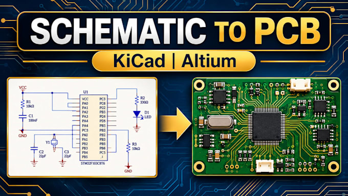
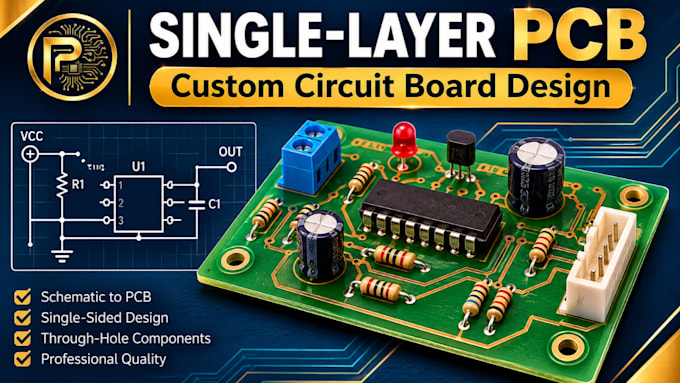
I design printed circuit board (PCB) layouts for electronic products, development projects and hardware prototypes. I can help turn circuit schematics into organized PCB layouts, including single-layer, double-layer and multilayer boards. My workflow focuses on component placement, practical routing and design-rule checks. Depending on the project scope, deliverables can include editable design files, Gerber files, drill files and a bill of materials (BOM).... Lees meer