Sommige informatie wordt in het Engels weergegeven.
Over mij
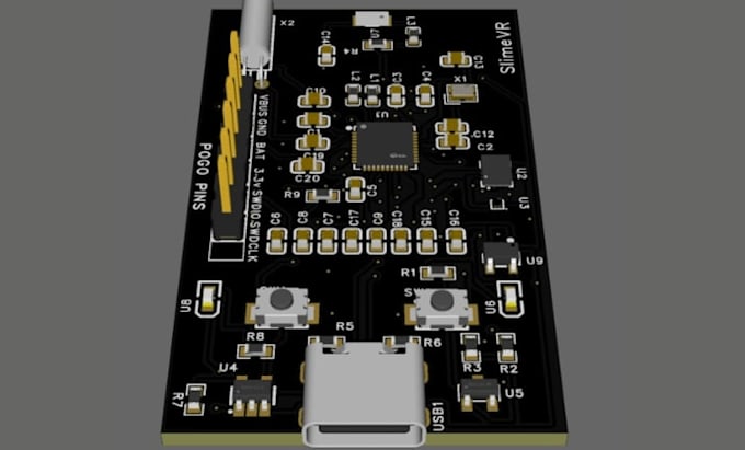
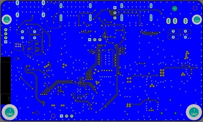
I'm a PCB design engineer focus in PCB layout, schematic design, RF PCB, multilayer PCB, high-speed PCB, and power electronics.
I design manufacturing ready PCBs with optimized routing, Gerber files, BOM, and DFM validation. My expertise includes DC-DC converters, SMPS, BMS, inverter PCB, impedance controlled layouts, and PCB redesign.
I also provide PCB review, schematic review, and manufacturing optimization to ensure reliability, performance, and production success. Using KiCad, Altium Designer, and EasyEDA, I deliver professional PCB solutions from concept to fabrication ready files.... Lees meer