Het lijkt erop dat deze dienst tijdelijk niet beschikbaar is

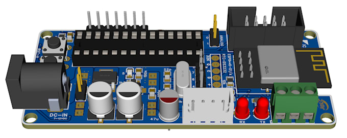
I will do professional or custom pcb layout design, and schematics layout in easyeda

Sommige informatie wordt in het Engels weergegeven.

Indonesië

Ik spreek Engels

DESIGNATOR

About Me I am an active university student with experience as a Network Administrator and Web Programmer. I specialize in web development, UI/UX and graphic design, PCB layout design, and computer ne...
Over deze dienst

Looking for a professional, reliable, and high-quality PCB layout? You are in the right place!

I am an experienced electronics designer specializing in custom PCB layout design and schematic capture using EasyEDA. Whether you have a rough hand-drawn sketch, a breadboard prototype, or a detailed component list, I will transform your ideas into a fully functional, production-ready printed circuit board.

What I Offer:

  • Custom & Professional PCB Layout (Single, Double, or Multi-layer)
  • Clean & Readable Schematic Diagrams
  • Component Selection & Footprint Creation
  • Gerber Files, Bill of Materials (BOM) with LCSC/Digikey parts, and Centroid Files for SMT Assembly
  • 3D PCB Rendering views

Why Choose Me?

  • Optimized for Manufacturing: Designs tailored for JLCPCB, PCBWay, or any fabrication house.
  • Signal Integrity: Proper routing, ground planes, and power trace widths.
  • Fast Delivery & Clear Communication.

Perfect for IoT devices, microcontrollers (ESP32, Arduino, STM32), DIY projects, or commercial hardware.

Please contact me before placing an order to discuss your project requirements! Let's bring your hardware to life!

Specialisatie:

Circuit design

Schema's

Lay-out

Voetafdruk

Gerber

Bestandsformaat:

Gerber

BRD

SCH

PDF

ODB

Software:

Eagle CAD

EasyEDA

KiCad

Interface:

HDMI

MIPI DSI/CSI

TDM

UART

USB

SPI

I2C

SDIO

Wi-Fi

BT

GSM/GPRS