Door categorieën bladeren
Ontdekken
Fiverr Pro
Nederlands
$
USD
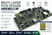
Looking for a professional PCB designer who can handle multi-layer boards with complex routing? I design clean, reliable, and manufacturing-ready 4, 6, and 8+ layer PCBs using EasyEDA, following professional PCB layout standards.
I specialize in high-density and multi-layer PCB designs, ensuring proper schematics, optimized layer stackups, clean routing, and layouts suitable for fabrication and assembly.
Whether youre building a high-speed digital board, embedded system, or complex control circuit, I focus on signal integrity, power distribution, and manufacturability.
What I offer:
Please contact me before ordering to confirm board size, layer count, and complexity.

Specialisatie:
Circuit design
•
Schema's
•
Lay-out
•
Analyse
•
Gerber
Bestandsformaat:
Gerber
•
STEP
•
BRD
•
SCH
•
Software:
EasyEDA
•
LTspice
•
Matlab
•
NI Multisim
How many layers do you support?
I support 4, 6, 8, and higher layer PCB designs.
Do you handle complex and high-density routing?
Yes, including high-speed signals and dense component layouts.
Will I receive manufacturing files?
Yes, Gerbers, BOM, and pick-and-place files are included.
Which software do you use?
EasyEDA for schematic and PCB layout.
