Door categorieën bladeren
Ontdekken
Fiverr Pro
Nederlands
$
USD
PCB ELEKTRISCHE ENGINEER EXPERT
HALLO EN WELKOM BIJ MIJN GIG!!!
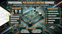
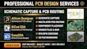
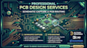
Ik voer professionele schematic capture en PCB routing uit in Altium Designer, KiCad en EasyEDA voor elektronische, embedded, IoT, automotive en industriële projecten. Of je nu een eenvoudige PCB, multilayer board, STM32-systeem of productieklare layout nodig hebt, ik lever schone, geoptimaliseerde en betrouwbare PCB-oplossingen die op jouw wensen zijn afgestemd.
Mijn service richt zich op nauwkeurige schema-ontwikkeling, efficiënte routing, signaalintegriteit, juiste componentplaatsing en fabricageklare outputs om een soepele PCB-productie en prestaties te garanderen.
Wat ik aanbied
Waarom voor mij kiezen
Stuur me gerust een bericht voordat je je bestelling plaatst om je schematic capture en PCB routing project in Altium, KiCad of EasyEDA professioneel te bespreken!!!
Automatische vertaling
Welke PCB-software ondersteun je?
Altium Designer, KiCad, EasyEDA en meer.
Lever je Gerber-bestanden?
Ja, fabricageklare bestanden zijn inbegrepen.
Kun je multilayer PCBs ontwerpen?
Ja, inclusief geavanceerde routing projecten.
Ondersteun je schematic capture?
Ja, schematic en PCB routing zijn inbegrepen.
Kun je routing en plaatsing optimaliseren?
Ja, voor prestaties en fabricage.


