Door categorieën bladeren
Ontdekken
Fiverr Pro
Nederlands
$
USD
PCB Designer for JLCPCB, KiCad and Gerber Fixes
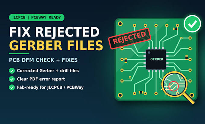
Was your PCB rejected by JLCPCB or PCBWay? I fix rejected Gerber files and run a PCB DFM check so your board passes fab review and gets manufactured without delays.
Ideal for startups, makers, hardware engineers and product teams who need production ready files fast.
I check your Gerber files, drill files and layout for the errors that cause rejections:
What you get:
How it works:
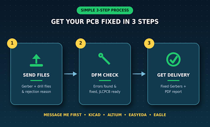
1. Message me before ordering with your files and the rejection reason.
2. I confirm scope, price and delivery time.
3. I fix, check and deliver your files.
I work with KiCad, Altium, EasyEDA and Eagle files.
Expect fast, clear communication and honest feedback and if a fix needs a design change, I tell you first.
Send your files today and get your PCB errors fixed fast, so your board ships to production without another rejection.


Why was my PCB rejected by JLCPCB or PCBWay, and can you fix it?
Common causes are trace width and spacing below the fab's minimum, small annular rings, drill sizes that are too small, and copper too close to the board edge. I check your Gerber files against JLCPCB and PCBWay capabilities, fix what can be fixed in the files, and list anything that needs change.
Which files do I need to send?
Send your Gerber files (RS-274X) and Excellon drill files, plus the fab's rejection message if you have one. For the BOM and CPL check on Premium, also send your BOM and pick and place (CPL) file. Original design files help too, but aren't required.
Can you fix solder mask, silkscreen and pad problems?
Yes. I check solder mask openings and expansion, silkscreen over pads, missing pads and wrong outlines. Some fixes are easier in the source design, so I'll tell you when the fix is safer in your original file than in the Gerbers.
Which design software do you support?
I work with files from KiCad, Altium, EasyEDA and Eagle. If yours comes from another tool, message me first and send the Gerbers so I can confirm I can check them.
Will my board definitely pass after your fix?
I can't promise the fab's own review will accept it, since each manufacturer has its own limits and can change them. What I do is check your files against their published capabilities and give you a report of every issue found and fixed. If a problem need a real design change, I'll let you know.