Sommige informatie wordt in het Engels weergegeven.
Over mij
PCB Design Engineer | From Schematic to Manufacturing Files
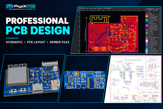
I design fabrication-ready 2-layer and 4-layer PCBs — schematic capture, PCB layout, Gerber files, BOM, Pick and Place files, and DFM/DRC checks.
Tools: KiCad, EasyEDA Pro, Proteus, MATLAB Simulink.
I focus on clean layout, signal integrity, and manufacturing-ready deliverables, so your board goes to fabrication without re-spins.
Message me with your schematic, board size, and requirements before ordering.... Lees meer