Sommige informatie wordt in het Engels weergegeven.
Over mij
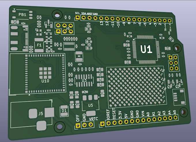
I am an Electronics Engineer & PCB Designer specializing in two-layer PCB design using KiCad.
I can assist with schematic capture, component selection and footprint assignment, PCB layout, component placement, routing, and preparation of manufacturing-ready Gerber and drill files.
I focus on creating clean, organized, and manufacturable PCB layouts while following design rules and component datasheets.
Services I Offer:
* 2-layer PCB design and routing
* Schematic capture and circuit-to-PCB conversion
* Reverse engineering PCB from Gerbers
Let's turn your circuit idea into a PCB!... Lees meer