Door categorieën bladeren
Ontdekken
Fiverr Pro
Nederlands
$
USD
PCB Design Engineer
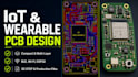
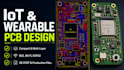
Are you an inventor, startup, or engineer looking to bring a smart gadget or wearable tracker to life? Generic PCB layouts often fail due to size constraints or signal noise. You need an expert who understands compact, low-power hardware.
I specialize in high-density, compact PCB design specifically for IoT and wearable devices. Whether you are using ESP32, STM32, nRF52, BLE, Wi-Fi, or cellular modules, I will design a high-performing, stable circuit board tailored to your enclosure.
What I Offer:
Click "Order Now" or message me with your block diagram to start building!
What inputs do I need to provide to start the project?
Please provide your detailed project requirements, a block diagram or hand-drawn schematic sketch, a component list (if you have preferred chips), and the physical dimension limits or enclosure constraints of your device.
Which EDA tools do you use for designing the PCBs?
I design professional-grade circuit boards primarily using Altium Designer, KiCad, or Autodesk Eagle, depending on your preferences. You will receive the native design files along with the standard production-ready assets.
Do you assist with low-power optimization for battery-operated wearables?
Yes, absolutely. Wearable tech relies heavily on battery life. I strictly implement proper power plane isolation, low-dropout regulators (LDOs), and optimal ground routing to ensure your circuit minimizes parasitic power consumption.


