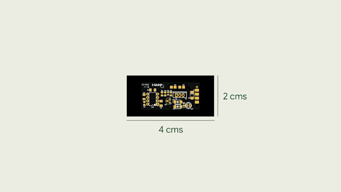
I will design a 2 layer pcb

Sommige informatie wordt in het Engels weergegeven.

India

Ik spreek Engels

Hardware And PCB Design Engineer

Hi, I'm a Hardware Design Engineer with 7+ years of experience turning ideas into production-ready electronics. I partner with founders and engineering teams globally to delivery reliable, first-time-...
Over deze dienst

Need a reliable, production-ready 2-Layer PCB designed in KiCad? I will take your schematic, circuit design, or concept and turn it into an optimized, manufacture-ready circuit board.


What I Offer:

  • KiCad PCB Layout: Precision placement, optimal routing, ground planes, and thermal considerations
  • Component Flexibility: Expert handling of both SMD and through-hole (THT) parts
  • Custom Layouts: Tailored to fit exact board dimensions, connector placements, enclosure constraints, or mounting requirements
  • Error-Free Verification: Thorough ERC/DRC checks to prevent costly manufacturing mistakes


Deliverables Included:

  • Full KiCad Source Files (Schematic & Board Layout)
  • Complete Manufacturing Package (Gerber & NC Drill Files)
  • Pick & Place / CPL Files for Automated Assembly
  • Professional Bill of Materials (BOM)
  • 3D STEP Model (if included in the purchased package)


Whether you need a prototype or a low-cost production board, I ensure your design is fully optimized for budget fabricators like JLCPCB and PCBWay.


Please click "Contact Seller" with your schematic or project notes before ordering so I can confirm your specs!


Specialisatie:

Circuit design

•

Schema's

•

Lay-out

•

Voetafdruk

Bestandsformaat:

Gerber

•

STEP

•

SCH

•

PDF

Software:

Altium ontwerper

•

EasyEDA

•

KiCad

Interface:

I2S

•

UART

•

USB

•

SPI

•

I2C

•

SDIO

•

Wi-Fi

•

BLE

•

BT

Mijn portfolio